The Model 7928A is a miniaturized, hermetically sealed PIN diode phase shifter covering the frequency range from 6 to 18 GHz providing a full 360° range of variable phase shift. It can also be used to perform frequency translation. The unit is an integrated assembly of an RF vector modulator and a driver circuit consisting of an 8-bit D/A converter and a voltage buffer. See Figure 1.
 Fig 1-Model 7928A, block diagram
PHASE SHIFT
Phase shifting is achieved utilizing the RF vector modulator approach shown in Figure 2. The 3-dB hybrid coupler divides the RF signal into two quadrature components which are then biased in proportion to the sine and cosine of the desired phase shift. The signals are then combined in-phase to yield desired output.
 Fig 2-RF Vector Modulator
ACCURACY
Improved phase accuracy and PM/AM performance are achieved by using double-balanced bi-phase linearamplitude modulators. In the main operating band, overall phase accuracy is better than 12°. The same phase accuracy can be achieved at the band edges byusing a built-in frequency correction circuit .Switching speed is better than 500 ns.
FREQUENCY TRANSLATION (SERRODYNING)
In the design of the Model 7928A special attention has been paid to those characteristics which affect its performance as a frequency translator. These include minimizing PM-to-AM conversion, use of high slew rate drivers, and optimizing phase shift linearity with applied signal. As a result, carrier and sideband suppression levels of over 25 and 20 dB, respectively, are obtained in the main band. The same carrier and sideband performance can be realized over the full stretch band when the internal frequency correction circuit is employed. See Fig. 3 for input control requirements. On special order, frequency translators can be provided for operation over reduced bandwidths with suppression levels of up to 40 dB. Consult the factory for such requirements.
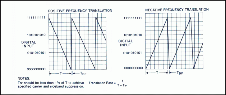 Fig 3-Model 7298A input requirements
Operating Note: To initialized the unit after power up, at least one of the digital bits has to change its TTL level.
| PHASE SHIFTER SPECIFICATIONS |
FREQUENCY RANGE (GHz)
|
INSERTION
LOSS (Max.)
|
VSWR (Max.) |
ACCURACY (Max.)
|
PM/AM (Max.)
|
Main Band 8.0-18.0
Stretch Band 6.0-18.0 (3)
|
12.0 dB |
2.0:1 |
±12°
±15°
|
±1.1 dB
±2.0 dB |
| FREQUENCY TRANSLATOR SPECIFICATIONS |
TRANSLATION RATE (Min.)
|
CARRIER (1) SUPPRESSION (Min.)
|
SIDE BAND SUPPRESSION (Min)
|
INSERTION LOSS
VARIATION (Max.)
with translation rate of: |
0 to 500 kHz (2)
|
Main Band: 25 dB
Stretch Band: 18dB (3
|
Main Band: 20dB
Stretch Band: 15 dB(3
|
200kHz: 1dB
500kHz: 3dB |
(1) When operating as a Phase Shifter outside the Main Band Frequency Range, a TTL Low (0) applied to the J3
Power/Control Connector Freq. Correction Pin (pin R) will result in Stretch Band Frequencies exhibiting
enhanced performance characteristics. The resultant Accuracy and PM/AM specifications will be the same as
those shown for the Main Band Frequency Range. When using the unit as a Frequency Translator, similar
enhanced performance can be achieved for Carrier & Sideband Suppression.
(2) All specifications are met using only the five most significant bits for translation rates of 0 to 200 kHz. For
translation rates of 201 to 500 kHz, only 4 most significant bits are used.
(3) Specification for the Stretch Band are typical
| PERFORMANCE CHARACTERISTICS |
| Phase Shift |
| Range ...................................................... |
360° in 256 steps |
| Variation .................................................. |
0.1°/C° |
| Control Input ........................................... |
8 bit TTL |
| Switching Speed ...................................... |
500 ns max (50% TTL to within 10° of Final Phase Value) |
| Harmonics ............................................... |
-30 dBc |
Power Handling Capability
Without Performance Degradation ............ |
+20 dBm |
| Survival Power ......................................... |
+30 dBm |
| Power Supply Requirements...................... |
+5V ± 5%, 80 mA max
+ 12 to 15V, 10 mA max
-12 to -15, 95 mA max |