Switch Application Notes
General Microwave Switches cover the frequency range from 100 MHz to 40 GHz and are available in various topologies ranging from single-pole single throw (SPST) to single-pole eight-throw (SP8T) in both reflective and non-reflective configurations, and a Non- reflective SP16T unit.
MICROWAVE SWITCHES TOPOLOGY
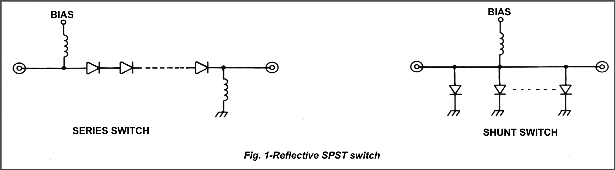
There are two fundamental methods of connecting PIN diodes to a transmission line to provide a switching function: in series with the transmission line so that RF power is conducted when the PIN diode is forward biased and reflected when reverse biased; or in shunt with the transmission line so that the RF power is conducted when the diode is reverse biased and reflected when forward biased. A simple reflective SPST switch can be designed utilizing one or more PIN diodes in either configuration as shown in Fig. 1.
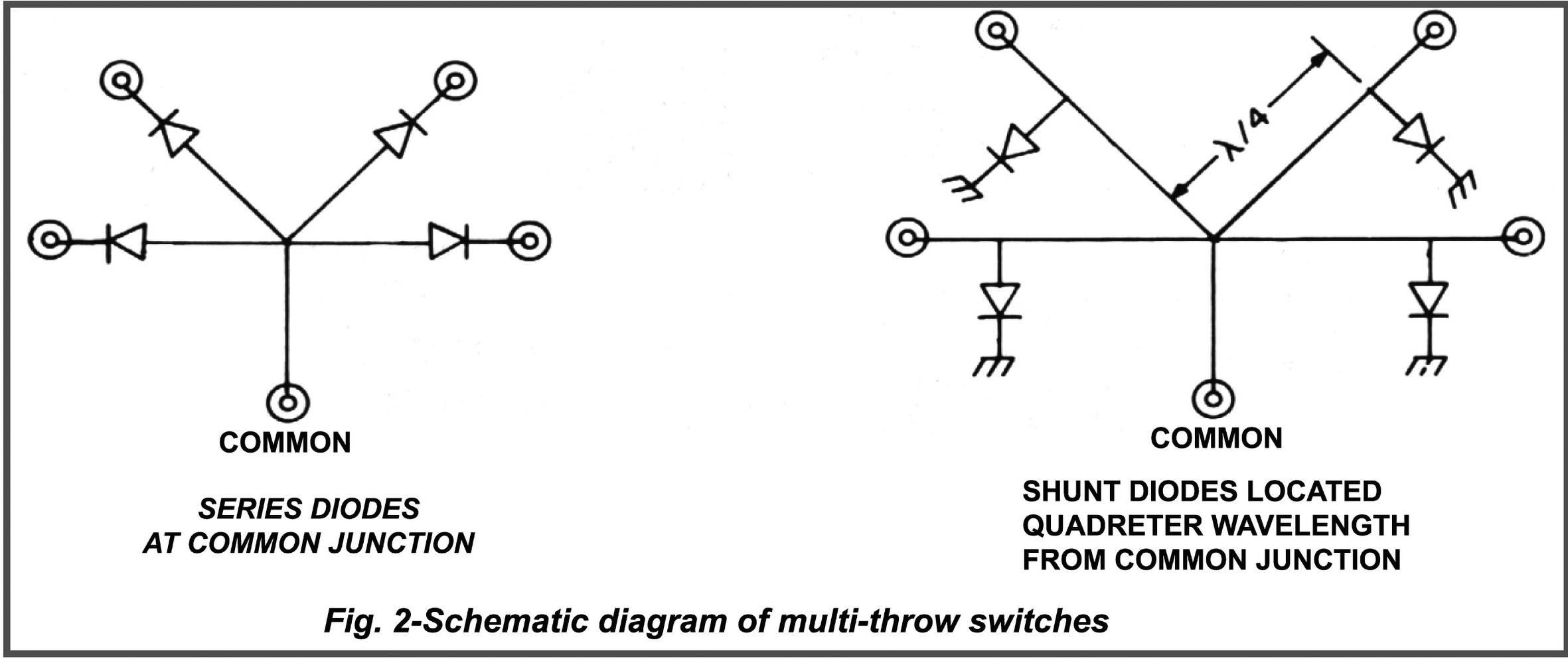
A multi-throw microwave switch essentially consists of combination of SPST switches connected to a common junction and biased so that each switch port can be enabled individually. The common junction of the switch must be designed to minimize the resistive and reactive loading presented by the OFF ports in order to obtain low insertion loss and VSWR for the ON port. There are two basic methods of realizing a multi-throw microwave switch common junction for optimum performance over a broad frequency range. The first employs series mounted PIN diodes connected to the common junction. A path is selected by forward biasing its series diode and simultaneously reverse biasing all the other diodes. This provides the desired low-loss path for the ON port with a minimum of loading from the OFF ports. The second method utilizes shunt mounted PIN diodes located a quarter wavelength from the junction. The diode(s) of the selected ON port is reverse biased while the OFF ports are forward biased to create a short circuit across the transmission line. As a result of the quarter wavelength spacing, the short circuits are transformed to open circuits at the junction. By proper choice of transmission line impedances and minimization of stray reactance it is possible to construct a switch of this type with low insertion loss and VSWR over a three to one bandwidth. The schematic diagrams for both switches are shown in Fig. 2.
ABSORPTIVE SWITCHES
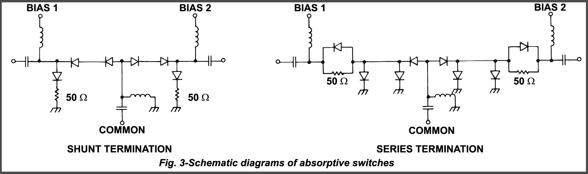
It is often desirable to have a PIN diode switch present a low VSWR in its OFF position as well as in its ON state in order to maintain desired system performance. Kratos General Microwave offers a complete line of single and multi-throw absorptive microwave switches which incorporate 50W terminations in each of the output ports. Fig. 3 shows the schematic diagrams of the two versions of absorptive (also known as Non-reflective or terminated) microwave switches employed by GMC. The shunt termination is used in GMC's "all-series" configured absorptive rf switches which have a suffix ending in “T” or “W”. This style of absorptive switch offers the minimum penalty in insertion loss due to the addition of the terminating elements. The series termination is used in GMC's high speed “series-shunt” configured absorptive switches since it provides the optimum in switching performance.
The common port of the standard absorptive multi-throw switches in the GMC catalog will be reflective in the special circumstance when all ports are turned OFF. If there is a need for this port to remain matched under these conditions, this can be realized either by employing an additional port to which an external termination is connected or, in a custom design, by providing automatic connection of an internal termination to the common port.
VIDEO LEAKAGE
Video leakage refers to the spurious signals present at the RF ports of the switch when it is switched without an RF signal present. These signals arise from the waveforms generated by the switch driver and, in particular, from the leading edge voltage spike required for high speed switching of PIN diodes. When measured in a 50 ohm system, the magnitude of the video leakage can be as much as several volts. The frequency content is concentrated in the band below 200 MHz although measurable levels for high speed switches are observed as high as 6.0 GHz. The magnitude of the out of band video leakage can be reduced significantly by the inclusion of high pass or “video filters” (1) in the switch. The Kratos General Microwave E-series switches are specially designed for low in-band video leakage, without sacrificing switching speed.
VIDEO FILTER OPTIONS
Applicability: F91 and G91 Switch Series
| |
Peak (mV) |
Bandwidth (MHz) |
| Video Leakage with Video Filter Options: |
100 max |
100 |
| INSERTION LOSS DEGRADATION |
| Option |
Affected Ports |
Frequency |
Additional IL |
| 41 |
Common Port Only |
1-12.4 GHz
12.4-18 GHz |
0.1 dB
0.2 dB |
| 42 |
Output Ports Only |
1-12.4 GHz
12.4-18 GHz |
0.1 dB
0.2 dB |
| 43 |
All Ports |
1-12.4 GHz
12.4-18 GHz |
0.2 dB
0.4 dB |
| VSWR DEGRADATION |
| Option |
Affected Ports |
Frequency |
VSWR |
| 41, 42, 43 |
All Ports |
1-4 GHz
4-18 GHz |
1.7 :1
No Change |
HARMONIC AND INTERMODULATION PRODUCTS
All PIN diode switches generate harmonics and inter-modulation products since the PIN diodes are fundamentally non-linear devices. The magnitude of these spurious signals is typically small in a switch since the diodes are usually either in their saturated forward biased state or in their reversed biased state. The physics of the PIN diode cause a cut-off frequency phenomena such that the level of harmonics and intermods greatly increase at low frequencies. These levels will vary with the minority carrier lifetime of the diode. Thus, a high speed switch operating below 500 MHz may have a second order intercept point of 35 dBm, while a slow switch operating at 8 GHz will have a second order intercept point of 70 dBm. Typical performance is as follows:
TYPICAL SWITCH INTERCEPT POINTS
| SWITCH |
FREQUENCY |
2nd Order
INTERCEPT |
3rd ORDER
INTERCEPT |
HIGH SPEED
LOW SPEED |
2.0 GHz
2.0 GHz |
+50 dBm
+65 dBm |
+40 dBm
+50 dBm |
Since these levels vary significantly with frequency, switching speed, and RF topology, please consult the factory for specific needs in this area.
PHASE AND AMPLITUDE MATCHING
Switches are available on a custom basis with phase and/or amplitude matching. Matching can be either between ports of a switch, between like ports on different switches, or a combination of the two. The uniformity of broadband catalog switches is quite good and is usually better than ±0.75 dB and ±15 degrees over the entire operating frequency of the switch. Please consult the factory for special requirements.
POWER HANDLING
The power handling of PIN diode switches is dependent on the RF topology, forward and reverse biasing levels, and speed of the switch. This catalog addresses both the maximum operating power levels and the survival limits of the components. Maximum operating limits are usually set at the power level which will cause the reversed biased diodes to begin conduction and thereby degrade the insertion loss, VSWR, or isolation of the switch. The survival power limits are based on the maximum ratings of the semiconductors in the switch. For special applications, significantly higher operational power levels can be provided, particularly for narrow band requirements. Please consult the factory for specific applications.
OPTION 55- EXTENDED FREQUENCIES
When Option 55 is applicable, a microwave switches in our catalog that covers 1-18 GHz can be modified to cover 0.5 to 18 GHz with following specification changes:
1. Specification for insertion loss and isolation from 0.5 to 1.0 GHz is the same as the 1-2 GHz specification. VSWR degrades to 2.0 :1.
2. Insertion loss in the 12.4-18 GHz band increases by 0.3 dB, Consult factory for cost.
DEFINITION OF PARAMETERS
INSERTION LOSS is the maximum loss measured in a 50 ohm system when only a single port of the switch is in the ON state.
ISOLATION is the ratio of the power level when the switch port is ON to the power level measured when the switch port is OFF. In a multi-throw switch the isolation is measured with one of the other ports turned ON and terminated in 50 ohms.
VSWR is defined for the input and output ports of the selected ON path. For those switches with a “T”, “W” or “HT” suffix, the VSWR is also defined for the OFF state.
SWITCHING SPEED(1)
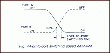
Port-To-Port Switching is the interval from the time the RF power level at the off-going port drops to 90% of its original value to the time the RF power level in the on-going port rises to 90% of its final value. See Fig. 4.
NOTE
(1) For a unit without an integrated driver, the specifications apply to conditions when it is driven by an appropriately shaped switching waveform.
Rise Time is measured between the 10% and 90% points of the square-law detected RF power when the unit is switched from full OFF to full ON. See Fig. 5.
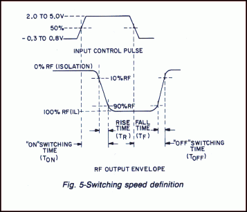
Fall Time is the time between the 90% and 10% points of the square-law detected RF power when the unit is switched from full ON to full OFF.
On Time is measured from the 50% level of the input control signal to the 90% point of the square-law detected RF power when the unit is switched from full OFF to full ON.
Off Time is measured from the 50% level of the input control signal to the 10% point of the square-law detected RF power when the unit is switched from full ON to full OFF.
In addition to the above definitions, the following information about switching performance may be useful to the system designer.
Switching To Isolation – Although catalog switching speed specifications are usually defined to the 10% level of detected RF (equivalent to 10 dB isolation), the user of microwave switches may be more interested in the time the switches requires to reach rated isolation. This latter time is strongly dependent on the topology of the switch. For all-shunt mounted or combination series and shunt mounted topologies, the time to reach final isolation is usually less than twice the fall time. For an all-series topology, the time to reach final isolation may be as much as ten times the fall time.
Switching To Insertion Loss – For multi-throw switches, the ON time depends on whether the switch is being operated in a commutating or single port mode. In the former mode, switching speed is slower than in the latter due to the loading effect at the junction of the port turning OFF. All switching speed measurements at GMC are performed in the commutating mode.
The information contained in this data sheet is basic marketing information and does not contain any export controlled information.