Microwave Attenuators: Application Notes
Request More Product Info |
Attenuator Selection Guide |
Switch Bit Attenuators Selection Guide
Kratos General Microwave PIN diode attenuators cover the frequency range from 200 MHz to 50 GHz and are available in numerous configurations to allow for system performance optimization. Most designs are available with either analog or digital control, operating over octave or multi-octave bands with high or moderate switching speed characteristics.
MICROWAVE ATTENUATOR TOPOLOGY
Kratos General Microwave PIN diode attenuator designs include several different topologies, each of which has is optimized for certain performance characteristics. A brief discussion of these various topologies is presented below including performance trade-offs.
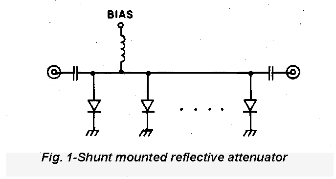
SHUNT-MOUNTED REFLECTIVE ATTENUATOR
The simplest version of a PIN diode attenuator consists of one or more PIN diodes in shunt with a transmission line as shown in Fig. 1. This design provides a broadband reflective attenuator that can reach very high levels of attenuation, depending upon the number and electrical spacing of the diodes. While it generally has very low insertion loss and can operate at high switching rates, its usefulness is limited by the very large mismatch it presents in the attenuation state.
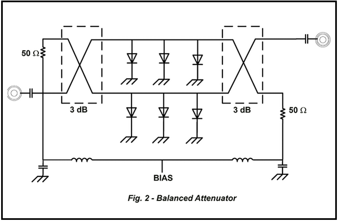
BALANCED ATTENUATOR
By placing identical shunt-mounted reflective attenuators between an appropriately connected pair of 3 dB quadrature hybrid couplers, a balanced attenuator is realized (see Fig. 2). The balanced attenuator has all the simplicity of the shunt-mounted reflective attenuator with the added feature of providing low VSWR under all conditions of attenuation. In addition, power handling is improved by 3 dB due to the power split of the input hybrid. This style of PIN diode attenuator offers simplicity, up to 3 to 1 bandwidth, moderately fast speed, and excellent linearity. Kratos General Microwave balanced attenuators cover the frequency range of 0.5 to 50.0 GHz.
ARRAY ATTENUATOR
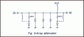
With the addition of terminating diode elements to the shunt-mounted reflective attenuators of Fig. 1, an attenuator can be realized with low VSWR that can operate over an octave band (see Fig. 3). By tapering the diode and transmission line impedance and adding multiple transformer sections it is possible to obtain good VSWR and attenuation characteristics over several octaves.
Kratos General Microwave employs array attenuators in a number of custom designs.
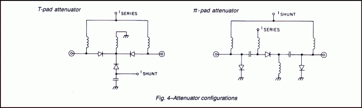
T-PAD AND π-PAD ATTENUATORS
The broadest frequency coverage available is obtained with some form of T-pad or π-pad attenuator. These are lumped element circuits which function in the microwave frequency range in essentially the same manner as they do at DC. Attenuation variation is obtained by simultaneously changing the bias current of the series and shunt diodes comprising the pads in a manner that assures constant impedance at all levels. Fig. 4 shows the basic configurations of both circuits. Only the T-pad configuration is used by GMC due to the difficulties in realizing sufficiently low stray reactances and short transmission line lengths in Π-pad circuits for operation at higher microwave frequencies. Models of these attenuators cover the full frequency range from 0.2 to 18.0 GHz with excellent attenuation lateness and moderate switching speed.
SWITCHED BIT ATTENUATORS
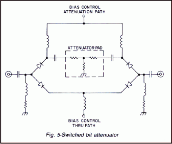
When an attenuator with a fast switching speed and high power handling capacity is required, the only option is to utilize a switched-bit attenuator. This attenuator combines one or more tandem pairs of SP2T switches with a zero loss connection between one pair of outputs and a ixed attenuator inserted in the other (see Fig. 5). In this configuration the PIN diodes are not used as variable resistors, but are switched between their forward and reversed biased states. This allows for much faster switching speed since high speed PIN diodes and drive circuitry can be used. In addition, it offers higher power handling capacity since the RF power is absorbed in the fixed attenuator(s), and not in the PIN diodes.
There are some disadvantages to this approach that may limit its usefulness. First, the minimum practical attenuation step size at microwave frequencies is about 0.5 dB due to interacting VSWR's as the bits are switched. These interactions may lead to a non-monotonic response as the attenuation is changed in increments of one LSB, i.e., the attenuation level may actually decrease when an increasing attenuation step is called for. Second, because of the RF circuit complexity, the cost of this attenuator is usually higher than other approaches. Finally, the incorporation of high speed switches may lead to excess video leakage.
PHASE INVARIANT ATTENUATORS
In this specialized class of attenuators, the insertion phase variation is minimized as the attenuation level is changed. A unique topology is employed by Kratos General Microwave to obtain this performance which is described in detail in a separate technical paper(1). In all other respects they perform in a manner similar to the balanced attenuators described above.
DRIVER CONSIDERATIONS
All attenuators except for the switched bit variety are available with linearizing driver circuits with either analog or digital control inputs. In addition, many attenuators are available without the driver for those who choose to provide their own. Most digital attenuators are available with eight-bit TTL control which, for an attenuator with a nominal attenuation range of 60 dB, will provide a resolution of 0.25 dB. Some attenuators are available with a resolution of as low as 0.05 dB. Except for switched-bit designs, all PIN diode attenuators are analog in nature and thus their resolution is essentially limited by the DAC used in the driver circuit.
The driver circuit includes compensating elements to minimize the variation of attenuator with temperature. It also provides the proper source impedance and switching waveforms to optimize switching speed.
STROBE/LATCH FEATURE - OPTION 4
lt is recommended that when operating the Series 349/H Attenuators with the Strobe/Latch Option -4 feature, the digital control inputs should be in place, with the Latch set to a low “(0)” level, before the Attenuator is powered up.
MONOTONICITY
In most applications it is imperative that the attenuator displays monotonic behavior as a function of the control input. Non-monotonic performance can occur in switched bit attenuators when interacting VSWR's are not properly compensated, or in digitally controlled analog attenuators when a non-monotonic condition exists in the MSB of the DAC. All GMC's attenuators are guaranteed monotonic.
PHASE SHIFT vs. ATTENUATION
All attenuators exhibit a variation in phase shift with attenuation level (AM/PM modulation). Fig. 6 shows typical phase shift variation as a function of attenuation for a number of GMC attenuator models. The phase shift is attributable to both the stray reactance of the PIN diodes as well as the lengths of transmission line interconnecting the diodes. While it is possible to minimize the AM/PM by careful design, it is not possible to eliminate it entirely. Where minimum change of phase with attenuation is a critical parameter, the use of GMC's line of Phase Invariant Attenuators described above should be considered.
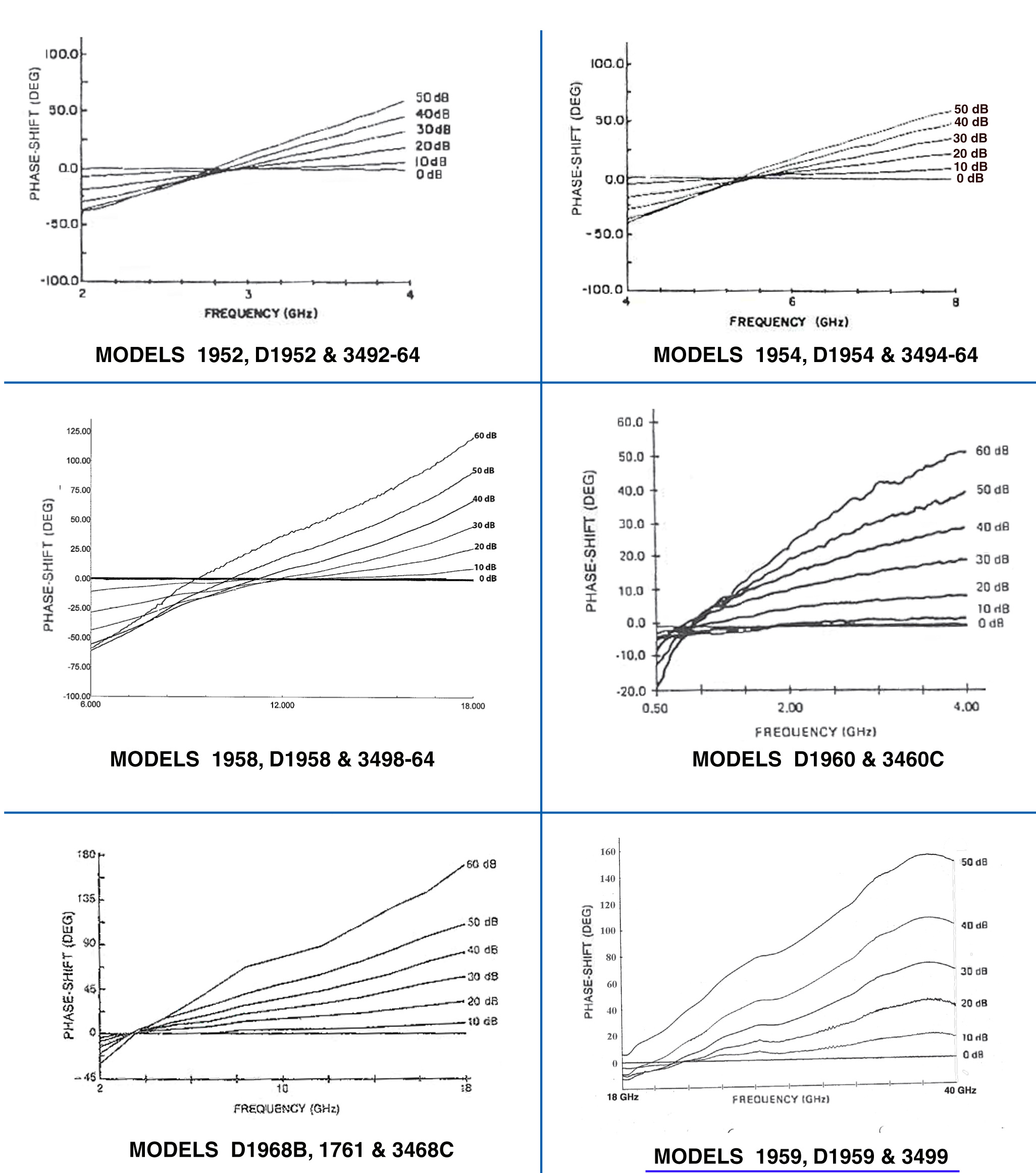
Fig. 6 - Typical Phase vs. Attenuation & Frequency
HARMONICS AND INTERMODULATION PRODUCTS
All PIN diode control devices (i.e. attenuators, switches and phase shifters) will generate harmonics and intermodulation products to some degree since PIN diodes are non-linear devices. When compared to digital switched-bit designs, analog PIN diode attenuators are more prone to generate spurious signals since the diodes function as current variable resistors and are typically operated at resistance levels where significant RF power is absorbed by the diode.
The levels of harmonic and intermodulation products generated by an attenuator are greatly dependent upon its design, the operating frequency, attenuation setting and input power level.
TYPICAL ATTENUATOR INTERCEPT POINTS
Typical performance for a moderately fast attenuator, i.e., 500 nsec switching speed.
FREQUENCY
|
2nd ORDER INTERCEPT
|
3rd ORDER INTERCEPT
|
2.0 GHz
8.0 GHz |
+ 35 dBm
+ 40 dBm |
+ 30 dBm
+ 35 dBm |
POWER HANDLING
The power handling of a PIN diode attenuator is dependent on its topology, biasing levels, and switching speed. The faster the attenuator, the lower the power handling capability. This catalog specifies both the maximum operating and the maximum survival levels. Maximum operating level is defined as the level which will cause an out of specification condition. The survival levels are generally dependent on the maximum ratings of the semiconductors in the attenuator. Please consult the factory for special applications requiring higher operational power levels than those listed in this catalog.
DEFINITION OF PARAMETERS
MEAN ATTENUATION is the average of the maximum and minimum values of the attenuation over the specified frequency range for a given control signal.
ATTENUATION FLATNESS is the variation from the mean attenuation level over the specified frequency range. This is usually a function of the attenuation level, and is expressed in ± dB.
ATTENUATION ACCURACY is the maximum deviation of the mean attenuation from the programmed attenuation value expressed in dB when measured
at + 23 ± 5°C.
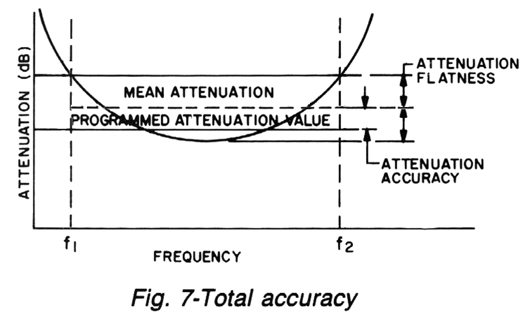 TOTAL ACCURACY is the sum of all the effects which contribute to the deviation from the programmed attenuation value. It includes the effects of attenuation accuracy, frequency variation and temperature, as shown in Fig. 7
SWITCHING SPEED(2)
The following are the standard definitions of switching speed, as shown in Fig. 8:
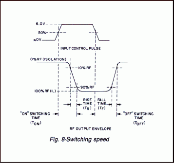
Rise Time is the transition time between the 10% and 90% points of the square-law detected RF power when the unit is switched from full OFF to full ON.
Fall Time is the transition between the 90% and 10% points of the square-law detected RF power when the unit is switched from full ON to full OFF.
On Time is the transition time between 50% of the input control signal to the 90% point of the square-law detected RF power when the unit is switched from full OFF to full ON.
Off Time is the transition time between 50% of the input control signal to the 10% point of the square-law detected RF power when the unit is switched from full ON to full OFF.
Note: Depending on the attenuator topology, there are differences in the behavior of the switching characteristics that may affect system performance. Switching speed is only specified to the 90% or 10% points of the detected RF signal, but the time the attenuator takes to reach final attenuation value or switch between different attenuation levels may be significantly longer.
MODULATION BANDWIDTH
Small Signal Bandwidth: With reference to a modulation frequency of 100 Hz and a modulation depth of ±3 dB at a quiescent level of −6 dB, the frequency at which the modulation depth decreases by 50% as measured with a square-law detector.
Large Signal Bandwidth: With reference to a modulation frequency of 100 Hz and a 100% modulation depth at a quiescent level of −6 dB, the frequency at which the modulation depth decreases by 50% as measured with a square-law detector.
TEMPERATURE COEFFICIENT is defined as the average rate of change of attenuation over the full operating temperature range of the unit under fixed bias conditions. It is expressed in dB/°C. Note that the attenuator temperature coefficient may vary with both temperature and programmed attenuation level.
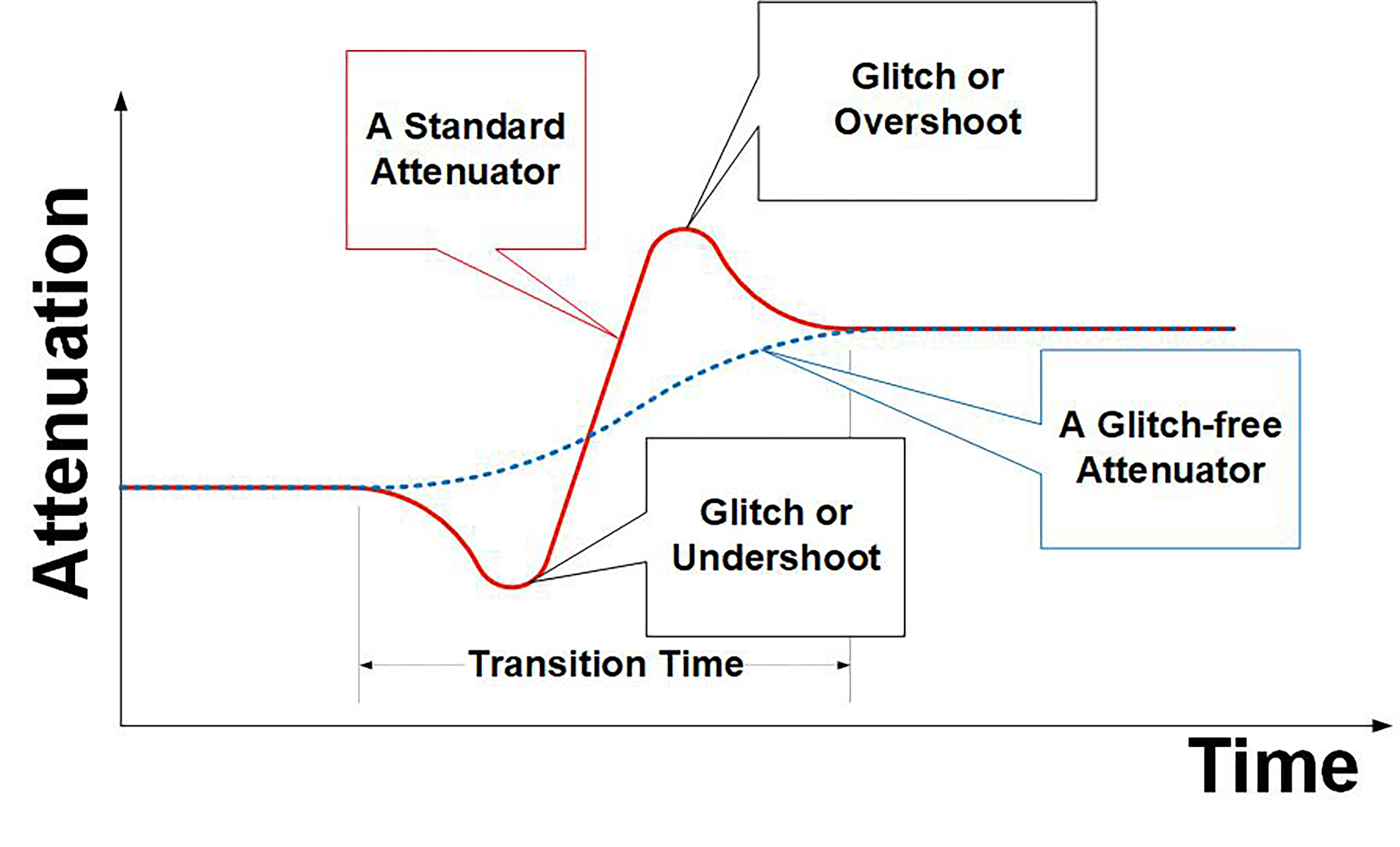
Glitch Free Driver – Option G10
With a standard attenuator driver, while the attenuator is in transition from value X to value Y, it can go through any arbitrary value of attenuation. This is sometimes called a glitch, sometimes an undershoot and sometimes an overshot. The “glitch free” attenuator is designed in such a way that the transition is smooth as possible from X to Y as illustrated in Fig. 9.
| |
 |
| |
Fig. 9 – Glitch free vs standard driver
|
The G10 option is recommended for new designs since it has only advantages and no penalties in performance or price.
NOTES
(1) “Broadband Phase Invariant Attenuator”, D. Adler and P. Maritato; 1988 IEEE MTT-S Digest, pp. 673-676.
(2) For units without integrated drivers, the specifications apply to conditions when the attenuator is driven by an appropriately shaped switching waveform.
Request More Product Info | Attenuator Selection Guide